Q2 Registers
All 48 register bits are implemented using positive-edge triggered D-flip-flops. These have the following structure:
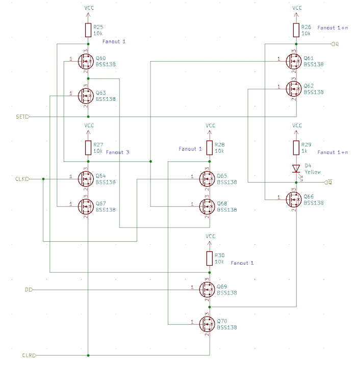
This is the classic NAND gate implementation of an edge-triggered flip-flop with a few modifications to save transistors. Note that the "SET" and "CLR" inputs have an inverted polarity when compared to the usual implementation.
The flip-flop includes an LED on the inverted output to show the state of the flip-flop. The voltage drop of this LED is important and must be kept small (here we assume 2 volts) to ensure proper operation at speed. A yellow LED is indicated here since red and yellow LEDs typically have low voltage drops.
Program Counter (P)
The program counter is made up of 12 flip-flops configured as a 12-bit binary ripple counter. Incrementing the program counter is accomplished by clocking the least-significant bit. To load the program counter, either for a jump or at reset, the set and clr inputs of the flip-flops are used.
Incrementing the program counter is slow since the clock has to ripple from the low bit up to the high bit, but the new value is not needed until a minimum of 7 clock cycles later, which is plenty of time.
Accumulator (A)
The accumulator is made up of 12 flip-flops configured as a shift register. Clocking the A register causes the output of the ALU to be shifted into the most significant bit (bit 11) and all lower bits to be shifted down one. The output of the least-significant bit (bit 0) is used as input to the ALU.
The A register can be read onto the data bus to execute the store instruction (STA).
Operand (X)
Like the accumulator, the operand register is made up of 12 flip-flops configured as a shift register. Rather than the output of the ALU, zeros are shifted into the X register. This detail is only important for the SHR instruction, making SHR perform a logical shift (a signed arithmetic shift would require copying the most significant bit instead).
To load the operand register, the high bits can be set to zero (zero-page loads), P (relative loads), the data bus (DBUS, for dereferencing), or shifted. The low bits can only be set to the data bus or shifted.
Opcode (O)
The opcode register is uses 4 flip-flops. It is loaded with the top 4-bits of the data bus during the FETCH state to save the operation to perform. The outputs of the opcode register along with the state register are used to control which operations to perform.
Because the program counter is incremented during the same state as the opcode register is written (FETCH), it is important that the opcode register is edge-triggered rather than a latch. It would be possible to move the increment of P to another state (perhaps sharing DEREF), but doing so would only save a few transistors and the layout of the Q2 makes it easy to implement these as flip-flops.
Flag (F)
The flag register is used to keep track of carries when doing addition during the ALU state and as a condition register for the jump flag clear (JFC) instruction.
Unlike many modern architectures with flag registers, the Q2 only has a single flag to represent multiple conditions (depending on the instruction). Not only does this reduce the number of flip-flops required, but it also saves space in the instruction encoding since only a single conditional jump is needed.
< Arithmetic Logic Unit | RAM >