Q2 Architecture
The Q2 is, in many ways, a 1960s-style minicomputer on a board. Inspired by the DEC PDP-8 (the PDP-8/S in particular), it is a 12-bit accumulator-based architecture with a small instruction set and a bit-serial ALU.
The Q2 was designed to keep the transistor count down while keeping the instruction set versatile enough to be usable. Unfortunately, this means the Q2 is fairly slow. All instructions take either 8 or 32 cycles to complete. Further, to keep the power consumption down without increasing transistor count, the maximum clock frequency is somewhere around 150 kHz. Higher frequencies should be possible at the expense of more power (lower valued resistor pull-ups) or more transistors (active pull-up). While slow even for a 1960s computer, the Q2 is still fast enough to run many interesting programs including those that require interaction, such as games.
The Q2 has three user-visible registers:
- A - 12-bit accumulator
- F - 1-bit flag
- P - 12-bit program counter
In addition to these, there is a 12-bit X register that is used to hold the operand, a 4-bit state counter, 1-bit clock divider, and a 4-bit opcode register. Two additional flip-flops are used for the I2C interface (SDA and SCL). These 48 registers are positive edge-triggered D flip-flops.
Instruction Set
All instructions are one 12-bit word and have the following bit pattern:
OOO D Z XXXXXXX
 \  \ \    \____ Operand
  \  \ \________ Zero Page
   \  \_________ Dereference
    \___________ Opcode
Here OOO is the opcode which determines the operation to perform, D is the dereference bit, Z is the zero-page bit, and XXXXXXX gives the low 7 bits of the operand. The high 5 bits of the operand are set to either the high bits of the program counter (if Z=0) or 0s (if Z=1). If the dereference flag is set, the operand is then loaded from memory (X = [X]).
The zero-page bit allows easy access to the first 128 words of memory. These locations can be used much like additional registers (similar to the PDP-8 or 6502). The prefix "=" is used to indicate a zero-page operand.
The dereference bit is used to allow indirect access to a memory location. This can be used to access memory on other pages or for array accesses. The prefix "@" is used to indicate indirect access. The dereference bit and zero-page bit can be used together to perform an indirect access through the zero page (prefix "@="). This is useful for storing a stack pointer in the zero page, for example.
Combined, the dereference and zero-page bits provide 4 address modes:
| DZ | Notation | Meaning |
|---|---|---|
| 00 | x | Current page relative |
| 01 | =x | Zero page relative |
| 10 | @x | Indirect through current page |
| 11 | @=x | Indirect through zero page |
The following instructions are supported:
| Opcode | Name | Flag | Description |
|---|---|---|---|
| 000 | lda | Z | Load: A = [X] |
| 001 | nor | Z | Not OR: A = A NOR [X] |
| 010 | add | C | Add: A = A + [X] |
| 011 | shr | C | Shift right: A = [X] >> 1 |
| 100 | lea | - | Load effective address: A = X |
| 101 | sta | - | Store: [X] = A |
| 110 | jmp | - | Jump: P = X |
| 111 | jfc | - | Jump flag clear: if !F: P = X |
The flag is set on carry (C), zero (Z), or left unchanged (-), depending on the instruction.
Front Panel
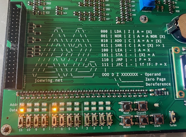
For programming, the Q2 has a simple front-panel interface. It has 12 LEDs to show the current address (the address bus, which is the P register after reset) and 12 LEDs to show the data bus. There are also 12 switches to serve as input and the following buttons:
- Deposit - Store the value in the switches to the current address.
- Next - Increment the P register (the current address).
- Reset - Set the P register to the value in the switches and reset the Q2.
- Stop - Stop the clock.
- Start - Start the clock.
The front panel allows one to enter a program and run it. However, the process is quite time-consuming and error-prone, so the front panel switches are also exposed through a 40-pin header. This header just happens to have a pinout that lines up with the GPIO pins of a Raspberry Pi, making it easy to use a Raspberry Pi to program and backup the Q2 via the q2prog utility. Note that Raspberry Pis with the 26-pin header will only be able to write to the Q2, but Raspberry Pis with a 40-pin header can both read and write.
Input/Output
The Q2 exposes the LCD, buttons, an I2C interface, and a memory extension device through address 0xFFF:
  Writes to 0xFFF:

      00 0 C DDDDDDDD
       \    \    \____ Data
        \    \________ 1 if a command, 0 for data
         \____________ LCD device

      10 C D 00000000
       \  \ \_________ SDA
        \  \__________ SCL
         \____________ I2C device

      11 0 0 0000000F
       \         \____ Field
        \_____________ Memory extension device

  Reads from 0xFFF:

      11 C D 111KKKKK
          \ \     \___ Keys (0 for pressed, 1 if not pressed)
           \ \________ SDA
            \_________ SCL
LCD and Buttons
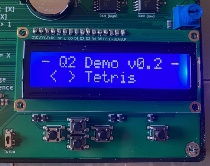
To allow one to interact with a running program, the Q2 includes a 16x2 LCD and five push buttons (older revisions had 12). The LCD and buttons are exposed via address 0xFFF. Reading from 0xFFF reads the current state of the buttons in the low 5 bits, where a 1 means the button is not pressed and a 0 means the button is pressed. The LCD uses the common HD44780 interface where the low eight bits are data/commands to the LCD and the 9th bit controls if data (0) or a command (1) is being written.
I2C Interface
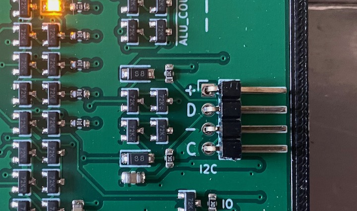
An I2C interface is provided to make it possible to connect sensors, EEPROM, etc. to the Q2. The SCL and SDA bits can be set by writing to 0xFFF with the top bit set. Bit 9 controls SCL and bit 8 controls SDA. Reads from 0xFFF return the state of the SCL and SDA bits. Note that I2C is an open-collector protocol, so SDA should be set high to enable reads.
Memory Extension
The memory extension device allows the Q2 to address more than 4096 words of memory. This is accomplished through the use of two additional latches: the data field (DF) and the instruction field (IF). Memory accesses for indirect loads or stores have the data field appended to the address. All other accesses have the instruction field appended.
On reset, both the data and instruction fields are set to 0. The data field can be set by writing 0xCXX to address 0xFFF (the field is ignored for I/O). This will set the data field to XX. The data field is copied to the instruction field when a jump takes place. Note that the current version of the Q2 has two fields (0 and 1).
See the Implementation Details for details on how the Q2 works.