Q2 Clock
Run Latch
The run latch controls whether the Q2 clock is enabled. The run latch consists of a pair of cross-coupled inverters (2 transistors). Pressing the "Stop" button pulls the STOP signal to ground and pressing the "Start" button pulls the START signal to ground causing the STOP signal to go high. The STOP signal is connected to RST through a diode, which has the effect of pressing "Stop" when the Q2 is reset.

Clock Generation
The clock for the Q2 is generated using a 3-stage ring oscillator with a variable delay. The output of the clock is fed through an inverter to reduce load on the oscillator and preserve the phase, which should be high when not running. To halt the clock, an additional transistor gates the first stage.

The clock is divided into two non-overlapping clock phases: a state clock (SC) and a write strobe (WS). The phases are generated using the CDIV flip-fop and two NOR gates. The SC clock is used to advance the state machine and the WS clock is used to clock the other flip-flops and write to memory. Having two phases simplifies writes to memory and I/O. Further, it allows the state machine to be implemented as a simple binary ripple counter (otherwise the ripple would cause glitches).

The starting sequence of clock phases looks like this:
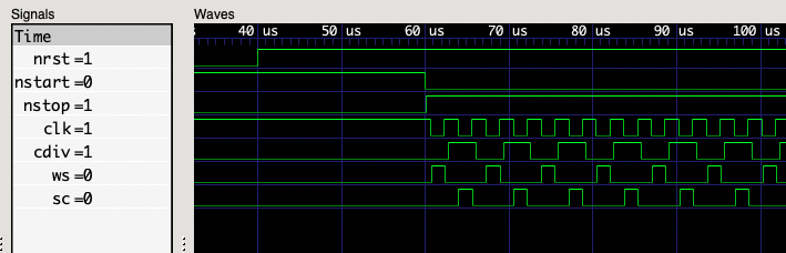
Here the Q2 powers up with the reset button pressed (nrst = 0). The reset button is released and then the start button is pressed to start the clock (nstart = 0).