Q1 State Machine
Contents
- Clock Generation
- Clock Phases
- Phase Transistion Logic
- States
- State Transistion Logic
- Class Decoder
- Function Decoder
- Control Lines
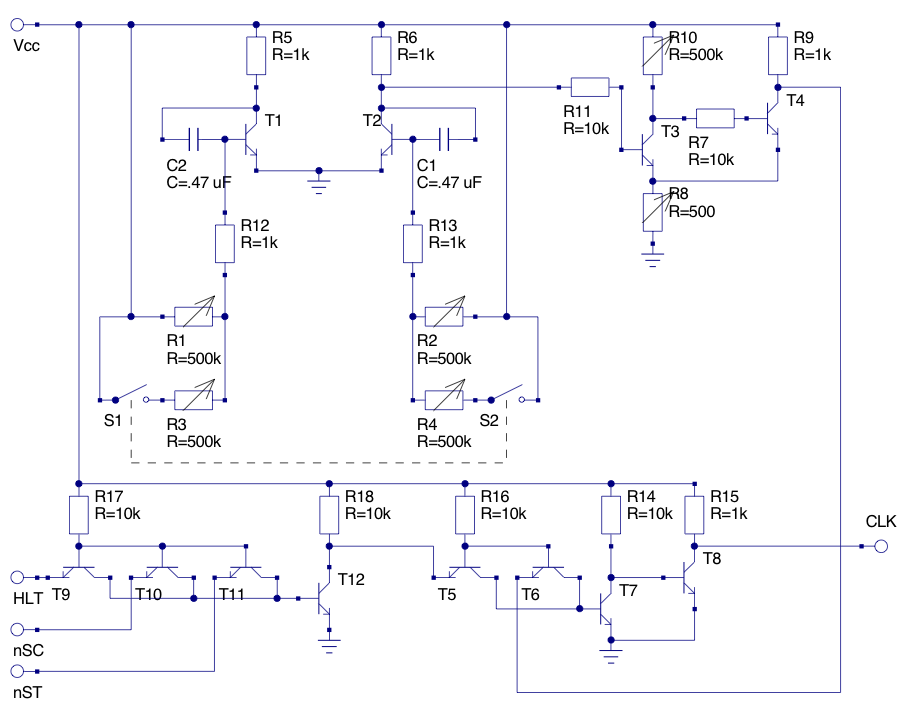
Clock Generation
The clock is generated by a 2-transistor astable multivibrator tied to
a Schmitt trigger.
Here's the schematic.
The output frequency is stable from about 30 Hz to 300 Hz, which could
easily be increased by using smaller capacitors.
12 transistors are needed.
Clock Phases
Each clock from the clock generator switches the clock phase on the
positive edge. Clock phases are used so that transparent latches can
be used for registers to reduce transistor count at the price of speed.
The state clock (SC) and write clock (WC) are generated from two positive
edge-triggered flip-flops with input from combinatorial logic.
The initial state is 00.
Each flip-flop requires 19 transistors (5 NAND2 gates and 1 NAND3 gate),
thus 38 transistors are required to keep phase state.
Asynchronous reset is accomplished by pulling the inverting output to
ground via an open-collector NOT gate for each flip-flop. Therefore,
the total transistor count is 42.
| Encoding | State Clock | Write Strobe | Next Phase |
|---|---|---|---|
| 00 | 0 | 0 | 11 |
| 11 | 1 | 1 | 10 |
| 10 | 1 | 0 | 00 |
Phase Transistion Logic
This is the logic used to compute the next clock phase.
Note that both inverted and non-inverted outputs are available as outputs,
but the input must be non-inverted.
7 transistors are needed for this logic.
| Signal | Logic | Simplified Logic | Gate Count | Transistor Count |
|---|---|---|---|---|
| P[1] | ~P[1] | P[0] | ~(P[1] & ~P[0]) | 1 NAND2 | 3 |
| P[0] | ~P[1] & ~P[0] | ~P[1] & ~P[0] | 1 AND2 | 4 |
States
Eight positive edge-triggered flip-flops clocked from the state clock are
used to keep the state. The next state is computed from combinatorial
logic.
The initial state is 1000 0000.
Each flip-flop requires 19 transistors plus 2 for reset. Thus 168
transistors are needed here.
| Encoding | Name | Description | Next State |
|---|---|---|---|
| 1000 0000 | sF1 | Fetch the opcode. | 0100 0000 |
| 0100 0000 | sP1 | Increment P. |
If C0 or C1: 0010 0000 Otherwise: 0000 0010 |
| 0010 0000 | sF2 | Fetch the first byte of the operand. | 0001 0000 |
| 0001 0000 | sP2 | Increment P. | 0000 1000 |
| 0000 1000 | sF3 | Fetch the second byte of the operand. | 0000 0100 |
| 0000 0100 | sP3 | Increment P. If this is a call instruction, X is written here. | 0000 0010 |
| 0000 0010 | EX | Execute. | 1000 0000 |
| 0000 0001 | HT | Halt. | 0000 0001 |
State Transistion Logic
Both inverting and non-inverting outputs are available, but the input
must be non-inverting.
31 transistors are needed here.
| Signal | Logic | Simplified Logic | Gate Count | Transistor Count |
|---|---|---|---|---|
| S[7] | S[1] & ~C3 & F8 | S[1] & ~C3 & F8 | 1 AND3 | 5 |
| S[6] | S[7] | S[7] | none | 0 |
| S[5] | (S[6] & C0) | (S[6] & C1) | ~(~(S[6] & C0) & ~(S[6] & C1)) | 3 NAND2 | 9 |
| S[4] | S[5] | S[5] | none | 0 |
| S[3] | S[4] | S[4] | none | 0 |
| S[2] | S[3] | S[3] | none | 0 |
| S[1] | S[2] | (S[6] & C2) | (S[6] & C3) | ~(~S[2] & ~(S[6] & C2) & ~(S[6] & C3)) |
1 NAND3 2 NAND2 |
12 |
| S[0] | S[1] & (C3 & F8) | S[1] & C3 & F8 | 1 AND3 | 5 |
Class Decoder
The class decoder determines the type of instruction stored in the
I (instruction) register. The I register provides constant inverted
and non-inverted outputs to make decoding easier.
24 transistors are needed here.
| Opcode | Class | Description | Size | Logic | Transistor Count |
|---|---|---|---|---|---|
| 0000 xxxx | C0 | Jump | 3 bytes | ~I[7] & ~I[6] & ~I[5] & ~I[4] | 6 |
| 0001 xxxx | C1 | Load/Store | 3 bytes | ~I[7] & ~I[6] & ~I[5] & I[4] | 6 |
| 0010 xxxx | C2 | Math | 1 byte | ~I[7] & ~I[6] & I[5] & ~I[4] | 6 |
| 0011 xxxx | C3 | Misc | 1 byte | ~I[7] & ~I[6] & I[5] & I[4] | 6 |
Function Decoder
The function decoder determines the ALU operation to perform for C2
instructions and the control lines to drive for C1 and C3 instructions.
Note that the logic for branching is handled separately for C0
instructions.
Both inverting and non-inverting outputs are provided
to make the control line decoder simpler.
63 transistors needed.
| Opcode | Function | Logic | Transistor Count |
|---|---|---|---|
| xxxx 0000 | F0 | ~I[3] & ~I[2] & ~I[1] & ~I[0] | 7 |
| xxxx 0001 | F1 | ~I[3] & ~I[2] & ~I[1] & I[0] | 7 |
| xxxx 0010 | F2 | ~I[3] & ~I[2] & I[1] & ~I[0] | 7 |
| xxxx 0011 | F3 | ~I[3] & ~I[2] & I[1] & I[0] | 7 |
| xxxx 0100 | F4 | ~I[3] & I[2] & ~I[1] & ~I[0] | 7 |
| xxxx 0101 | F5 | ~I[3] & I[2] & ~I[1] & I[0] | 7 |
| xxxx 0110 | F6 | ~I[3] & I[2] & I[1] & ~I[0] | 7 |
| xxxx 0111 | F7 | ~I[3] & I[2] & I[1] & I[0] | 7 |
| xxxx 1000 | F8 | I[3] & ~I[2] & ~I[1] & ~I[0] | 7 |
Control Lines
This drives the 22 control lines for the computer. Due to the
number of transistors needed, it is split across two modules.
The first module controls lines 0 through 12 inclusive. The second
module drives lines 13 through 21 inclusive (including the TB line).
119 transistors needed for the first module.
116 transistors needed for the second module.
| No | Name | Logic | Transistors |
|---|---|---|---|
| 0 | rd_A_d |
~(~(EX & C1 & F8) $ ~(EX & C3 & F0) $ ~(EX & C3 & F1) $ ~(EX & C3 & F2)) |
17 |
| 1 | wr_A_alu | EX & C2 & WC | 5 |
| 2 | rd_B_d |
~(~(EX & C1 & F4) $ ~(EX & C3 & F3)) |
9 |
| 3 | wr_B_d |
~(~(EX & C1 & F0 & WC) $ ~(EX & C3 & F0 & WC) $ ~(EX & C3 & F5 & WC)) |
16 |
| 4 | rd_C_d |
~(~(EX & C1 & F5) $ ~(EX & C3 & F4)) |
9 |
| 5 | wr_C_d |
~(~(EX & C1 & F1 & WC) $ ~(EX & C3 & F1 & WC) $ ~(EX & C3 & F6 & WC)) |
16 |
| 6 | rd_XH_d | EX & C1 & F6 | 5 |
| 7 | wr_XH_d | EX & C1 & F2 & WC | 6 |
| 8 | rd_XL_d | EX & C1 & F7 | 5 |
| 9 | wr_XL_d | EX & C1 & F3 & WC | 6 |
| 10 | rd_X_a |
(EX & C3) $ ~(~F2 & ~F3 & ~F4 & ~F5 & ~F6 & ~F7) |
11 |
| 11 | wr_X_a | sP3 & C0 & TB & I[3] & WC | 7 |
| 12 | rd_P_a | ~(~sF1 $ ~sF2 $ ~sF3) | 7 |
| 13 | wr_P_a |
~(~(sP1 & WC) $ ~(sP2 & WC) $ ~(sP3 & WC) $ ~(EX & C0 & TB & WC) $ ~(EX & C3 & F7 & WC)) |
20 |
| 14 | rd_N_a | ~(~sP1 $ ~sP2 $ ~sP3) | 7 |
| 15 | wr_N |
~(~(sF1 & WC) $ ~(sF2 & WC) $ ~(sF3 & WC)) |
10 |
| 16 | wr_I_d | sF1 & WC | 4 |
| 17 | rd_O_a |
~(~(EX & C0) $ ~(EX & C1)) |
7 |
| 18 | wr_OH_d | sF2 & WC | 4 |
| 19 | wr_OL_d | sF3 & WC | 4 |
| 20 | mem_rd |
~(~sF1 $ ~sF2 $ ~sF3 $ ~(EX & C1 & (~I[4] $ ~I[5])) $ ~(EX & C3 & F5) $ ~(EX & C3 & F6)) |
21 |
| 21 | mem_wr |
~(~((EX & C1 & WC) $ ~(~F4 & ~F5 & ~F6 & ~F7 & ~F8)) $ ~((EX & C3 & WC) $ ~(~F2 & ~F3 & ~F4))) |
23 |
| - | TB |
~(I[7] & ~CF) $ ~(I[6] & ~ZF) $ ~(I[5] & ~NF) |
16 |